
Home > SMT Assembly News
Circuit board or printed circuit board (PCB) or printed wiring board (PWB), is a board made out of non-insulating and highly heat-resistant insulating material such as fiberglass. These boards are also called substrates. A substrate or board may have only one single layer (single-layer circuit board) or more than one layer (multilayer circuit board). A conductive metal such as copper is used to make conductive pathway or traces to facilitate flow of electricity. Once these conductive traces are etched on the substrate, it is termed as “printed circuit board”.
History of Printed Circuit Board
The history of circuit boards dates back to mid-1930s, when an Austrian engineer Paul Eislerinvented the PCB while designing a radio set. These radio sets were later massively used in World War II by United States. After this, the use and application of circuit boards because commercial in electronics industry. These circuit boards are of no good use until electronic components are soldered. Electronic components can be either through-hole or SMD. Again the technology used to solder these components on the circuit board can be through-hole technology or surface mount technology. Soldering material may include solder in the form of solder wire, solder paste, solder balls for BGA (ball grid array) and solder flux.
Circuit Board Design: Guidelines, Rules and Tools
As explained above, a printed circuit board is a board made of one or more layers of insulating material (fiberglass, ceramic, highly heat-resistant plastic or any other dielectric material) with conductive pathways etched with metal such as copper. During the manufacturing process of the circuit board, traces of copper or any other conductor is etched off the board leaving only traces that are needed to mount / solder electronic components. Once all electronic components are soldered on the circuit board and the board is ready for use, it is called printed circuit assembly (PCA) or printed circuit board assembly (PCBA).
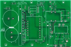
PCB or Printed Circuit Board
The current generic standard for design of a circuit board is IPC-2221A. IPC 2221A generic standard on printed board design provides rules for manufacturing circuit boards and quality guidelines. These information and guidelines is applicable for all types of circuit boards including single-layer and multilayer PCBs and information includes substrate information, material properties, criteria for surface plating, conductor thickness, component placement, dimensioning and tolerance rules and more.
Other circuit board designing standards are IPC-2220 and IPC-9592. It has to be noted that IPC and other standards will provide information on how to properly route the board.
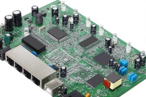
PCBA or Printed Circuit Board Assembly
For a perfect and reliable circuit board design, good knowledge and understanding of PCB layout techniquesand basic understanding of circuit operation is needed. While designing a printed circuit board prototype, one must take proper care of the substrate material based of type of soldering technology and components to be used. The width of the traces of the circuit board (circuit conductors) should be chosen wisely based on expected maximum temperature rise at the rated current and acceptable impedance. Other points to keep in mind with circuit board design are CTE, cost and dielectric properties. The designer needs to carefully balance the constraints of cost with reliability and performance needs. In addition, solder masks and via holes should also be selected carefully.
Printed Circuit Board Diagram
A circuit diagram is a diagram showing and explaining how and where electronic components will be mounted to achieve the target product. Each component on a circuit board diagram is represented by a symbol. Making a circuit diagram prior to production is critical. It gives an idea of how the circuit will work and how to achieve the target product. A circuit diagram is essential for any new electronic product, device or gadget.
How to draw a circuit diagram?
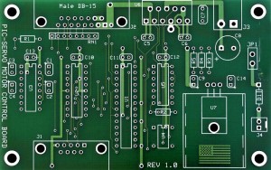
PCB Layout
Drawing a circuit diagram is not that difficult if you know the basics. Here are some tips and guidelines:
Printed Circuit Board Assembly
Mounting electronic components on the circuit board and getting it ready for use is what is called circuit board assembly. A Circuit board assembly process may use through-hole assembly technology or surface mount technology (SMT) or a mix to both. Once the circuit board is assembled with components it is ready for testing and finally to be assembled with the product. But it is not guaranteed that a circuit board assembly will give 100% zero defect production. There will be defects and these defect need to be reworked / repaired.
Keywords:
SMT Reflow Oven, Lead free Reflow Oven, Reflow Oven Manufacturer, LED reflow oven, PCB Reflow Oven, Nitrogen Reflow Oven, Dual Rail Reflow Oven, China Reflow Oven, wave soldering machine, Dual Rail Wave Soldering Machine, Nitrogen Wave Soldering Machine, Wave Soldering Machine Manufacturer.


Contact: Mr Tommy
Phone: +86 13691605420
Tel: +86 -755-85225569
Email: tommy@flason-smt.com
Add: 94#,Guangtian Road,Songgang Street,Bao an District Shenzhen China