
Home > Industry News
A Semiconductor can be defined as a material that has the characteristics and ability to conduct a small amount of electrical current. Semiconductors have much lower resistance to the flow of electrical current in one direction than in another. Electronic Components such as Diodes, transistors, and many photovoltaic cells contain semiconductive materials. The electrical conductivity of a semiconductor device can be controlled over a wide range, either permanently or dynamically.
Which Materials are used to make a Semiconductor?
There are several materials that are used to make a semiconductor. The basic requirement of a semiconductor is that it should not be a very good conductor of electricity, nor should it be a very bad conductor of electricity. Its properties can be changed by adding or removing atoms. Siliconis the most widely used semiconductor material. Few other materials used in making semiconductor are germanium, gallium arsenide, and silicon carbide.
How are Semiconductors Made?
Manufacturing semiconductors need expertise and experience. Chemicals to be used need to be pure and free from any impurity. The process of adding controlled impurities to a semiconductor is known as doping. Silicon wafers are an important ingredient in manufacturing semiconductors.
Semiconductor Manufacturing Process:
How Semiconductor Works
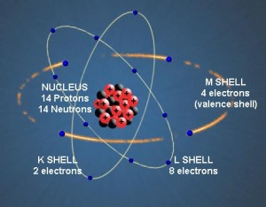
How Semiconductor Works
All semiconductor materials like silicon, germanium, gallium arsenide, and silicon carbide have a unique property – All of them have 4 electrons in their outermost orbit. All the 4 electrons form perfect covalent bonds with four other atoms creating a lattice to form crystals. These crystals may look like a diamond (if the semiconductor material used is carbon) or it may look like a silver metallic substance (if the semiconductor material used is silicon).
Most semiconductors are made by using silicon since it is abundantly available on earth and is easy to work with. When an “impure” substance, such as boron or gallium is introduced in small quantity, it causes the silicon crystal to become unstable. This instability allows free movement of electrons. Free movement of electrons causes an imbalance of electrons. This imbalance of electrons can generate a charge which can be either a positive charge (if there are lesser electrons) or a negative charge (if there are more electrons).
Conclusion
Silicon is the most widely used semiconductor material. Electrons are negatively charged and protons are positively charged while neutron has no charge. Semiconductors works due to imbalance of electrons that carry negative charge. This imbalance of electrons generates positive (where there are excess protons) and negative charges (where there are excess electrons) at two ends of surfaces of the semiconductor material. This is how a semiconductor works.
Keywords:
SMT Reflow Oven, Lead free Reflow Oven, Reflow Oven Manufacturer, LED reflow oven, PCB Reflow Oven, Nitrogen Reflow Oven, Dual Rail Reflow Oven, China Reflow Oven, wave soldering machine, Dual Rail Wave Soldering Machine, Nitrogen Wave Soldering Machine, Wave Soldering Machine Manufacturer.


Contact: Mr Tommy
Phone: +86 13691605420
Tel: +86 -755-85225569
Email: tommy@flason-smt.com
Add: 94#,Guangtian Road,Songgang Street,Bao an District Shenzhen China