
Home > SMT Equipment News
2D AOI Technology
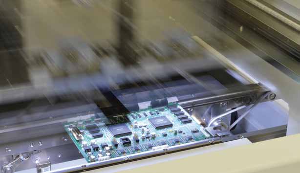
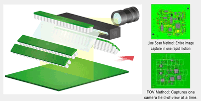
2D AOI systems use pixel reflections from the surface of the PCB, components, solder, and other PCB structures to perform image analysis and determine the existence and location of features on the surface of the PCB assembly. 2D technology is also employed in 3D AOI systems.Saki's Line Scanning Technology Changed the GameIn March 1995, Saki launched its first 2D automated optical inspection (AOI) system to check the surface of printed circuit boards and the tops of the components. Saki's unique system was based on Line Scanning Technology--a proprietary, high-speed imaging technology which scans an entire printed circuit board assembly (PCBA) and captures its image, on-the-fly, in just one pass, similar to the way a copy machine scans a document. This revolutionary technology increased the speed of the inspection process by 55%.Saki's PCB inspection method projects multiple lights at different angles onto the substrate while obtaining multiple images in one scanning operation. Saki's highly developed optical system realizes high resolution while also sustaining a high signal-to-noise (S/N) ratio. Resolution is important because the greater the resolution the better the ability to detect signals that are extremely close together for the sharpest and most detailed images. Often, to get high resolution, you have to compromise S/N. That's not the case with Saki's technology.
Line Scanning Technology still forms the basis of Saki's 2D systems and Saki is still known for its innovative, high quality, high speed inspection systems.Saki's 2D InnovationsMemory Technology: With Saki's memory technology, our machines capture all the parts on the substrate in one view, whether they are large connectors or microchips such as 0402 and 0603 parts. Board capture is not dependent on the size of the field of view (FOV). This information is used instantly to create inspection data of the entire board.Coaxial Overhead Lighting
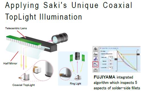
Coaxial overhead lighting creates an image for every field of view without using directed lighting and without creating the shadows that usually result from light deflected by taller components on the board. Overhead lighting is essential for proper inspection of microchips located between connectors on high density boards and is effective for solder fillet inspection that is dependent on the relationship between the tilt angle and brightness. With coaxial overhead lighting, inspection data can be applied to similar components, facilitating inspection data management, and speeding up production start-up.
Large Diameter Telecentric LensWhen combined with Saki's line scanning technology, the telecentric lens captures a sharp image from above.Digital Shading CompensationSaki's digital shading compensation corrects luminance in real time during scanning to avoid uneven brightness and aberrations within the pixels. Used in combination with our multiple lighting systems, uneven brightness is corrected and image distortion is eliminated within a broad view of 1500 megapixels. The result is superior reproducibility, reliability, consistency, and compatibility between machines.Double-sided Inspection
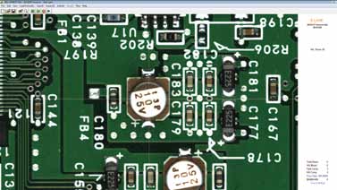
Saki's line scanning technology uses a simple one-axis structure and low vibration so both sides of the board can be inspected simultaneously. This is especially beneficial for final confirmation after selective soldering of defective components. The machine's compact footprint and safety features support easy installation into a production line or production cell configuration.Double-sided Simultaneous Inspection: In Saki's unique double-sided simultaneous inspection system, one AOI machine provides the function of two. Both sides of the board are inspected simultaneously to cut inspection time almost in half. It avoids mishandling, reduces the number of operations needed, and eliminates the need for a board flipper.Fujiyama AlgorithmSaki's unique Fujiyama algorithm verifies five critical aspects of through-hole solder joints, thereby providing thorough inspection of through-hole solder joints to ensure quality for not only SMT solder joints, but for all solder joints in mixed technology applications. Saki's FUJIYAMA algorithm enables solder inspection after wave soldering to check for extra components, dropped components, stray components, and solder balls.ECD (Extra Component Detection)Saki's ECD (Extra Component Detection) algorithm inspects for stray components, solder balls, and foreign materials across the entire surface of the circuit board and can detect objects of 300 microns or less, thereby eliminating these defects. ECD provides further assurance of product quality. Saki's ECD is incorporated into both its 2D and 3D AOI systems.Complete Surface Inspection—reference board comparisonLine scanning technology captures the image of the entire board, not individual images that have to be pieced together, so it can easily detect incorrectly placed or missing parts, excessive or foreign material, solder balls, or damage to the substrate. Images can be quickly and easily compared to a reference board, and reference board images can be easily updated for any changes to the board. 
1 - Selectable resolution (X-Y), 10µm or 20µm
2 - 250 x 330mm in dual-lane mode; up to 460 x 330mm in single-lane mode
* All AOI machines can be configured for Automated Conformal Coating Inspection (AOI)
* Conformal Coating Inspection
All Saki 2D AOI machines can be configured for automated conformal coating inspection. When the machine is ordered, Saki's BF-10Z, BF-10D, BF-Tristar II, BF-Planet-X II, BF-Frontier II, BF-10BT, BF-Comet10/18, and BF-Sirius can be equipped with conformal coating inspection capabilities.
After conformal coating installation on the BF-10BT, PCB clearance will be changed from both a top and bottom clearance of 40mm (1.57 in.), to a top and bottom clearance of 30mm (1.18 in.) from the PCB surface.
When a PCB's thickness and warp are 1mm (0.04 in.), the top clearance is 28mm (1.10 in.) and the bottom clearance is 30mm (1.18 in.) from the PCB.
Keywords:
SAKI AOI, SAKI 2D AOI, SAKI 3D AOI, Omron AOI, Omron 3D AOI, SMT AOI, PCB quality inspection AOI, China AOI, AOI manufacturer, SMT AOI manufacturer, SMT AOI supplier.


Contact: Mr Tommy
Phone: +86 13691605420
Tel: +86 -755-85225569
Email: sales@flason-smt.com
Add: No.94,Guangtian Road,Songgang Street,Bao an District Shenzhen China